By applying thin deposition, lithography and electroplating processings, various metal circuit and fine trace patterns can be manufactured on the surface of ceramic / Si substrate. Ceramic / Si substrate consists of various superior physical properties like thin dimensions, anti-corrosive, high temperature resistant…etc. Combining thin film lithographic processing & stable properties of ceramic, A lot of Applications can be achieved.
ICP has already set up the complete processing capability for the following products: thin film ESD suppressor, thin film resistor, thin film LED ceramic heat-sink and thin film inductor.
ICP can also provide customized thin film processing including:
Design & processing of Al2O3 substrate metallization & Patterning
Design & processing of AlN substrate metallization & Patterning
Design & processing of Si substrate metallization & Patterning
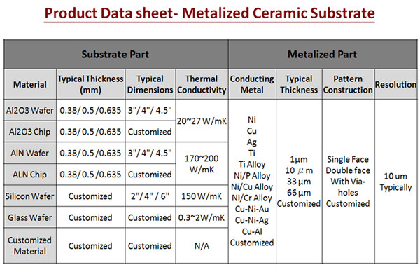
SPEC: